Below is our recent interview with Dr Filip Granek, CEO of XTPL:

Q: Could you provide our readers with a brief introduction to XTPL?
A: XTPL is a technology provider – a company that has developed a unique approach to printing various materials. Our additive manufacturing, ultra-precise method allows to obtain conductive & non-conductive structures on the individual micron scale (1-8 μm). We want to empower global electronics manufacturers by implementing this solution on their production lines. XTPL vision entails using the traditional advantages of print – such as scalability, lower cost, simplicity and speed – in the production of advanced, high tech devices. Our technology responds to the market need of progressing miniaturization and at the same time provides a cost-effective & scalable method. We believe that as easily and inexpensively as you print books and newspapers today, soon you’ll be able to print display, semiconductor or smart glass elements. The highest precision, one that will allow for this process to materialize, is what XTPL brings to the table.
Q: Why is your solution a breakthrough?
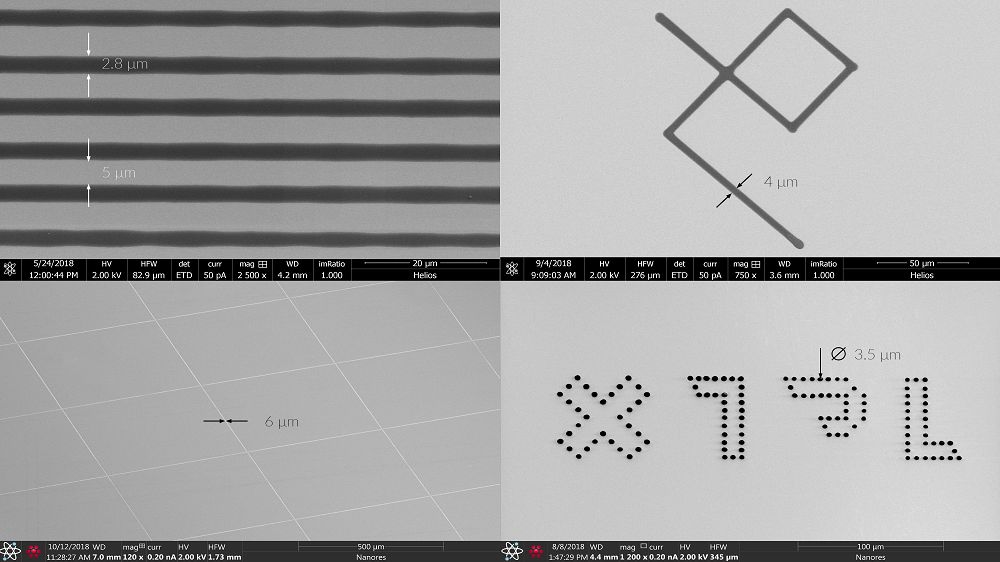
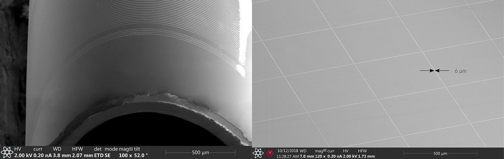
A: What makes XTPL solution unique is the unparalleled precision & versatility. This disruptive solution works on most substrates, conductive and non-conductive, as well as flat and 2.5D, such as glass, silicon wafers, kapton, PEN, PC, PDMS, PET. It can provide straight lines, as well as patterns and microdots. Our method allows for printing a large variety of available materials: conductive inks, nanoparticle based suspensions, semiconductor based suspensions, insulating inks, resists, solvent based inks and biological materials. In order to achieve outstanding results at XTPL we create our own nanoink formulas based mostly on metallic nanoparticles (Ag, Au and Cu) and semiconductors (TiO2). There is no electric field required for printing, which fully eliminates the risk of damage to the substrate and other electrically active components. Parameters & features of individual structures created with this method as well as the distance between them depend on the specific application requirements.
 Recommended: Skye Multimedia Develops Interactive Training That Keeps The Attention Of The Learner And Maximizes Retention
Q: Why is now the time for a technology solution like XTPL?
A: Modern electronics sector faces now a strong trend to produce high-tech devices using cost-effective and scalable methods. We have the unique technology to enable that advance. We like to think that our solution may potentially bring a true technological revolution. One could compare this process with previous revolution caused by the invention of printing press in 15th century. Although books have been around for nearly 3,000 years, they were rare and hard to manufacture until Gutenberg constructed this – then breakthrough – device. Before that text and illustrations were done by hand in a time-consuming process, and only the wealthy could afford them. But within a few decades Gutenberg’s innovation spread, which allowed literacy to flourish. Thanks to XTPL nanoprinting, the access barrier to technologically advanced devices will drastically decrease – they will become more effective and cheaper at the same time. And this may entail a number of positive social and economic changes. Our dream is the future, in which the comparison to Gutenberg, whose invention revived the circulation of thoughts in Europe and contributed to the popularization of new ideological movements and trends, will not be an exaggeration. This is the vision of the future that drives us.
Q: What are the key applications for XTPL technology?
A: Our solutions of nanoprinting my be applied in many sectors, mostly within printed electronics, e.g. in semiconductors, smart glass, advanced PCBs, anticounterfeiting or biosensors sector. Our key focus at the moment is flat panel display market. Here we have already verified serious competitive advantages of our technology. We are open to collaboration with display equipment manufacturers as well as display manufacturers themselves, to provide for them a high performance solution dedicated for industrial implementation. Hopefully we will be able to connect to the main players from this sector at the upcoming Display Week exhibition 14-16 May in San Jose (XTPL booth number 431).
Q: Since the display sector is the one you chose as your key focus for now what is the added value you bring to the table here?
A: Display sector faces some challenges: progressive complexity of displays occurring with reducing feature size, constant miniaturization causing yield issues on the advanced manufacturing lines, expensive, complex, limited & slow yield improvement (repair) methods, need for mechanical flexibility of new generation displays or electrical field damage risk – to name some of them. XTPL plans to support manufacturers in overcoming those issues.
For example the feature size of printed structures is one of the key parameters of our additive technology. XTPL solution can provide structures on the individual micron scale, which enables higher pixel density of the finished products. In particular the resolution, brightness and lifetime parameters of the final display are improved.
Another challenge faced by the modern FPD manufacturing lies in the fact that ultra-fine conductive structures are prone to damage. This is a major factor contributing to the decrease of the production yield. XTPL advanced additive method for open defect repair (ODR) responds to manufacturers requirements in this respect. It requires no electric field for printing, thus eliminating fully the risk of damage to the substrate and other electrically active components (non-electrostatic alternative to the EHD technology). Furthermore it allows for repairing broken conductive lines already at the production stage, which contributes to reduced takt time. Our method is effective and enables high spatial density of the printed features, high adhesion to the substrate (various options possible), all that with lower production cost for the manufacturers and no toxic substances used in the repair process.
Currently a strong trend for producers who aim to meet the customers’ expectations is the introduction of flexible displays. Due to the high production costs and low yield of flexible electronics, its introduction on a mass scale proves to be a challenge. XTPL offers solution that enables mechanical flexibility of new generation displays because electrically conductive structures obtained using our method retain their properties – including excellent electrical conductivity parameters – throughout the deformation of the substrate.
 Recommended: GradeBuddy Provides A Platform For Students To Access The Best Study Materials
It is also worth mentioning that due to the highest transparency of our structures and above mentioned excellent electrical conductivity parameters as well as mechanical flexibility XTPL solution can potentially be applied as an alternative also in transparent metal mesh manufacturing.
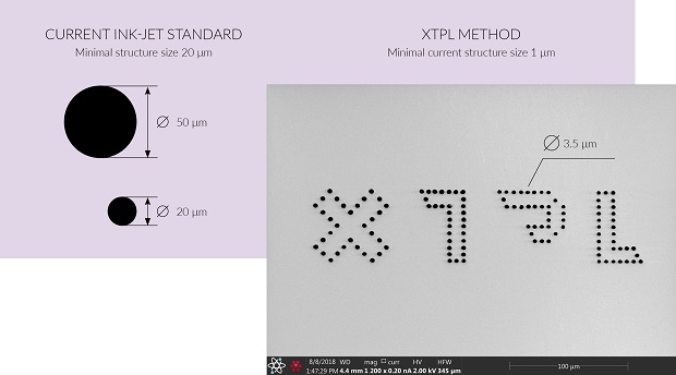
XTPL technology can be potentially used in the future also in OLED manufacturing to precisely deposit organic materials. Unlike the currently used fine metal mask (FMM) approach, structures obtained with our printing method do not exhibit shadowing effect with the increase of display size. This advance allows for reduced feature size irrespective of the scaling. Since our solution is purely additive, no organic material is wasted and there is no need for masks that have to be replaced between the deposition cycles. Currently used state-of-the-art ink-jet printers for the OLED industry deposit structures with a minimal diameter of 20 μm, while XTPL technology provides microdots as small as 1 μm in diameter. Additionally, the implemented XTPL ultra-precise deposition (UPD) allows for obtaining arbitrary shapes on any kind of substrate currently used in OLEDs.
 Recommended: Damo Consulting – Growth Strategy And Digital Transformation Advisory Firm
XTPL additive technology is also well suited for Colour Filter (C/F) deposition during the manufacturing or repair stages of the OLED and LCD panel production process. Universality of our method allows for the deposition of a wide range of possible C/F materials as well as sizes and does not require any masking.
Q: What are your plans for the future?
A: Short-term, we are constantly optimizing our technology and adapting it to various implementation requirements. We aim to build partnerships and strategic alliances with well-established partners within dedicated sectors – at the moment with strong focus on flat panel display market – and to cooperate in the form of joint development or technology transfer. The first natural direction for us is Silicon Valley. Mostly due to the concentration in this area of companies that are the leaders of the most interesting – for XTPL – sectors. At the same time, it is a market with a unique business infrastructure and vast experience in implementing high technologies. This was one of the reasons for opening our branch office in the Valley in February this year.
Long-term we know that as pioneers we are to implement new solutions on the global market, but to achieve this we need to build a certain awareness, be able to give our technology the right narrative, build it in a sustainable way – also in a broader social context. XTPL technology has one basic advantage – it is ground-breaking and therefore has a chance to replace existing, expensive and ineffective solutions. We hope that it will further facilitate the use of innovation for people all over the world.